Shared foundry runs or Multi-Project Wafers are a cost effective foundry approach well suited for Institutes, Labs, Research Centers and Universities. This service allows different customer projects on a single wafer.
You will be able to:
Participants have free access to Design Kits. 20 diced & untested MMICs in Gel-Pak® box will eventually be delivered.

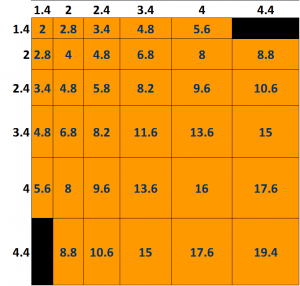
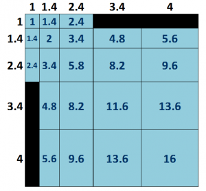
The possible die length and width, including dicing streets, are:
with maximum aspect ratio 1:3
with maximum aspect ratio 1:3


Price is determined according to die area and process.
UMS shared foundry runs offer regular Multi Project Wafer runs with information 6 months notice before tape-out.
Shared foundry runs 2022
Next low-medium power process runs
Next High Power Process run:
Next GaN Hemt process runs
Shared runs are scheduled based on customer needs. UMS optimize schedule to meet tape-out date that maximize delivery time agreement with customers.
Contact us @ tmtnanjing@163.com

地址:中国南京市玄武区龙蟠路155号紫金联合立方5幢 邮编:210037
电话:+86-25-84812008 ; 传真:+86-25-84812098 ; 电邮:tmtnanjing@163.com

